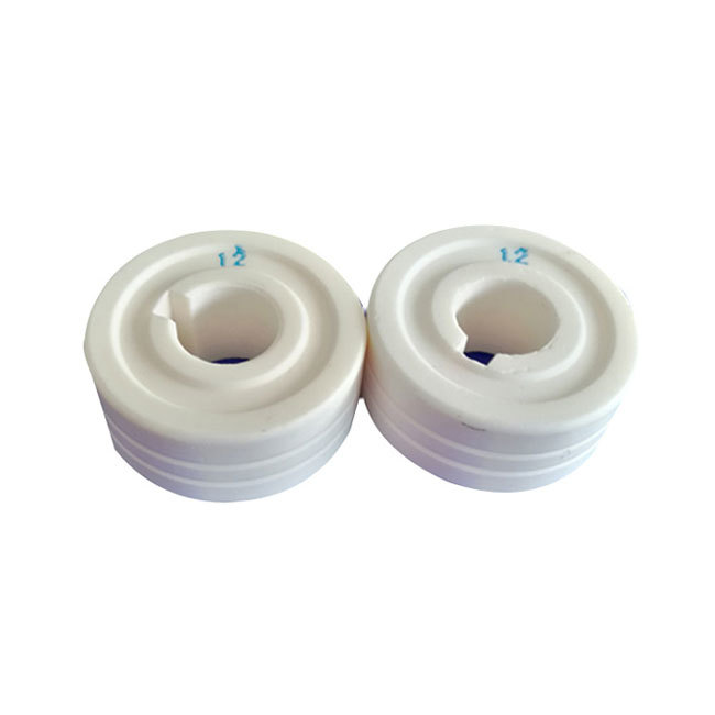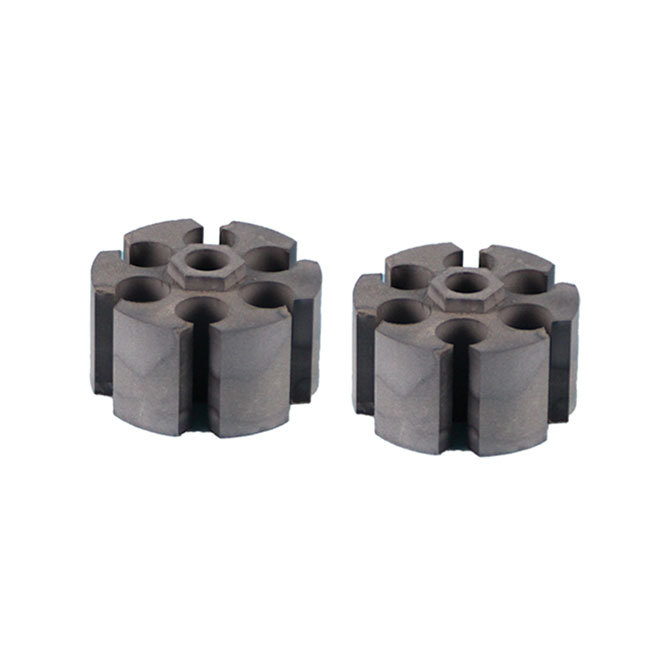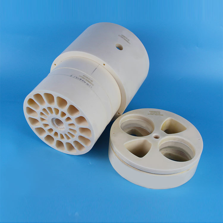
Round special ceramic
keywords:
Aluminum oxide ceramics, silicon nitride ceramics, zirconia ceramics
Category:
Product Details
The reason why ceramic substrates can occupy a favorable position in the field of high-power packaging is that special ceramic substrates have made breakthroughs in application innovation in technology, and it is just the right time to understand and analyze the pain points of thermoelectric separation special ceramic substrate technology.
What special ceramic substrate? The reason why it is also called direct copper-plated ceramic substrate is because the thin-film metal beverage electroplating technology uses image transmission to make metal lines, and then uses perforated electroplating technology to form high-density double-sided wiring and vertical interconnect holes.
The material of the special ceramic substrate is alumina ceramic with high thermal conductivity. If you want to go higher, you need to use aluminum nitride, which has a high thermal conductivity of 170. The thermal conductivity of aluminum alloy reaches 220~230. In other words, it is similar to metal and has high dielectric strength, making it a very good material. The higher the power, the better the performance of the aluminum nitride ceramic.
The use of special ceramic substrates is due to the recent continuous upgrading of LED technology and the improvement of LED light efficiency. The photoelectric conversion rate on high-power LED chips is only 70% to 80%, which means that 20% to 30% of the power is converted into heat. . The heat will definitely transfer. In fact, the main method is to use PCB for transmission. But it will be found that the heat conduction channel on the back of the chip is very heat conductive. This is the material used for the heat conduction channels.
The current solution is to directly fix the chip on the copper heat sink, but the copper heat pin itself is the conduction channel. That is, thermoelectric separation does not occur at lighting levels. The light source needs to have an insulating layer on the packaged PCB board for thermal and electrical isolation. If the heat is not concentrated on the chip, but concentrated near the insulating layer under the light source, once more power is generated, there will be heat dissipation problems. Therefore, special ceramic substrates can solve this problem by directly fixing the chip on the ceramic, forming vertical interconnection holes on the ceramic, and forming internal independent conductive channels. Ceramic itself is an insulator and can dissipate heat, so thermoelectric separation can be performed at the lighting level, so the PCB does not need to consider the thermoelectric separation structure, and there is no need to make heat insulation materials on the PCB.
Key technology of diphenyl carbonate ceramic substrate
1. The bonding strength between the metal circuit layer and the ceramic substrate
Since the thermal expansion coefficients of metals and ceramics are very different, in order to reduce the interface stress, it is necessary to add a transition layer between the copper layer and the ceramics to improve the interface bonding strength. The bonding force between transition layer and ceramics is mainly diffusion adhesion and chemical bond, so Ti, Cr, Ni and other metals with high activity and good diffusivity are often used as transition layer (also used as electroplating seed layer).
2. Plating and filling holes
Electroplating hole filling is also a key technology for the preparation of special ceramic substrates. At present, the plating holes of DPC substrates mostly use pulse power supply, and its technical advantage is that it is easy to fill the through holes and reduce the plating defects in the holes. The surface structure of the coating is dense and uniform in thickness. High current density plating can be used to increase deposition efficiency.
Message


